Google splits its TPU line to chase training and inference at hyperscale
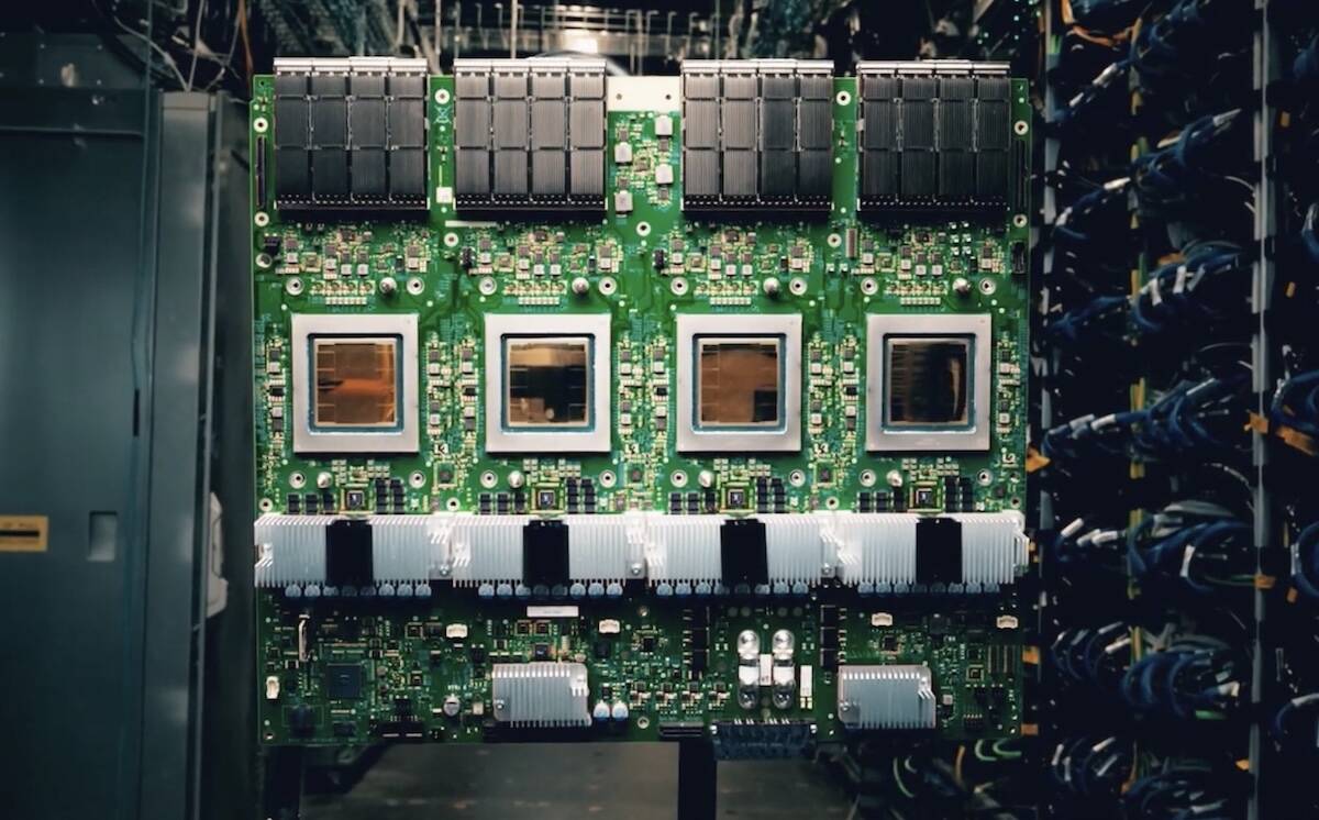
Google used Cloud Next 2026 to redraw its AI silicon strategy, unveiling separate TPU 8 chips for training and inference as it tries to win the next phase of the AI infrastructure race against Nvidia.
Key takeaways · 4
- 01
AI infrastructure is splitting into two economic problems: training frontier models and serving them cheaply at scale.
- 02
Inference cost and latency are becoming the decisive constraints for agentic products, not just model quality.
- 03
Google is betting that custom silicon plus tighter networking can offset Nvidia’s chip-by-chip performance lead.
- 04
The real differentiator may be pod-scale system design, not individual accelerator specs.
Why Google split TPUs
Google’s announcement is best understood as an admission that AI workloads no longer fit neatly inside one accelerator design. The company says TPU 8t and TPU 8i are built for the “agentic” era, where systems move beyond answering questions and start taking actions [2]. That shift matters because agentic products create persistent inference demand, which changes the center of gravity from model training to model serving [5][8].
The split also reflects a broader pattern across the industry. Amazon recognized early that training and inference reward different optimizations, and Nvidia has increasingly tuned Blackwell and Blackwell Ultra toward serving efficiency rather than only training muscle [1][8]. Google is now making the same bet in a more explicit way, treating the two phases as separate businesses with separate bottlenecks. In practice, that means memory hierarchy, interconnect, and power draw matter more than a single benchmark headline.
For AI teams, the strategic takeaway is straightforward: chip evaluation is becoming workload-specific. A model lab cares about time-to-train and cluster scaling, while a product team cares about cost per request, tail latency, and how much throughput can be sustained under real user traffic. Google’s dual-track TPU strategy is a signal that those tradeoffs are now decisive, not secondary [2][5].
Training gets a bigger pod
TPU 8t is Google’s training-focused chip, and the company is framing it as a scale product rather than a standalone processor. Google says a TPU 8t superpod can connect 9,600 chips, deliver 121 exaflops of compute, and pool 2 petabytes of shared high-bandwidth memory [4]. The Register’s read of the hardware adds more color: each accelerator is said to carry 216 GB of HBM, 6.5 TB/s of bandwidth, 128 MB of SRAM, and up to 19.2 Tbps of chip-to-chip bandwidth [1].
Those numbers matter less as a raw spec sheet than as a systems strategy. Google claims the new training chip is up to 2.8 times faster than Ironwood for training and roughly three times better on compute per pod [1][2][3]. It is also leaning on topology, not just silicon, to get there: the company has described new networking arrangements designed to reduce scaling losses across large clusters [1]. In other words, TPU 8t is meant to win when thousands of accelerators need to behave like one machine.
That is where Google’s scale advantage becomes interesting. Nvidia’s Rubin-class GPUs may outrun TPU 8t in per-chip performance, with higher FP4 training throughput and more HBM capacity on paper [1]. But Google is betting that frontier model training is won by pod design, not chip vanity metrics, and that a broader unified fabric can squeeze more effective work out of each deployment. If that holds, the market may reward the platform that scales most cleanly, not the chip that looks best in isolation.
Inference becomes the profit center
If TPU 8t is about raw compute density, TPU 8i is about the economics of running AI every day. Google says the inference chip delivers 80 percent better performance per dollar than last year’s Ironwood TPU, with 288 GB of HBM, 384 MB of on-chip SRAM, and doubled inter-chip bandwidth at 19.2 Tb/s [4]. Google and Business Insider both tie that design to the memory wall: inference is increasingly limited by how quickly a chip can fetch data, not just how fast it can compute [5].
That is especially relevant for agents. An agentic system may not just generate text; it may retrieve context, reason over it, call tools, and produce multiple intermediate steps before returning an answer. Each of those steps is an inference event, and each one incurs cost, latency, and energy usage [5][8]. Google’s pitch is that 8i’s bigger SRAM and faster interconnect make those repeated operations cheaper and more responsive, which is exactly what production agents need.
The company is also making a power argument, not just a speed argument. Google says both TPUs can deliver up to twice the performance per watt of Ironwood and rely on fourth-generation liquid cooling [4]. That echoes a larger industry shift: inference is now a budget line item, and the winners will be the vendors that can reduce cost per token, cost per request, and cost per useful action. On that front, Google is racing Nvidia on the same terrain, but with a very different hardware stack [5][8].
The moat is the system
Google’s TPU story is not just about the chips themselves. The company is pairing TPU 8 with Axion, its Arm-based CPU host, and ditching x86 for the control plane in the process [1][4][5]. It is also building the systems layer around the accelerators: AI Hypercomputer, distinct cluster topologies for different workloads, and a managed storage stack that includes Managed Lustre for AI training and serving [1][4]. The architecture suggests Google sees inference and training as full-stack problems, not socket-level problems.
The most ambitious part is the fabric. The Register reported that Google is using optical-circuit switching to connect up to 9,600 accelerators in a single pod and then stitching multiple pods together with its Virgo network [1]. That approach is aimed at reducing scaling penalties across massive compute domains, with claimed connectivity across 134,000 TPUs in a datacenter and even larger multi-site constructs [1]. Whether every number survives real-world deployment is another question, but the direction is clear: the network is part of the accelerator.
This full-stack approach is also what makes Google a different kind of competitor. Nvidia sells the best-known silicon and increasingly bundles software around it, but Google can design the CPU host, cooling, storage, scheduling, and network around its own chips [8][9]. That creates a tighter optimization loop, especially for customers already using Google Cloud. It also means Google can sell TPU-based infrastructure while still supporting Nvidia-based workloads on the same cloud, which makes the competitive boundary less clean and potentially more durable [5].
A direct Nvidia challenge
The customer list may be the most revealing part of the story. Techi reported that Anthropic, Meta, and now OpenAI are all taking multi-gigawatt TPU allocations, with OpenAI being the notable signal because it has long been treated as an anchor Nvidia customer [3]. If true, that suggests the market is no longer assuming frontier AI must run exclusively on Nvidia silicon. Google’s TPU business would then move from internal tool to external platform.
That does not mean Nvidia is suddenly weak. Techi notes that data center revenue still dominates Nvidia’s mix, with hyperscalers accounting for more than half of that demand [3]. But diversification among hyperscalers is exactly how monopoly premiums erode: first unit growth slows, then pricing power follows. Google’s claim that TPU 8i delivers 2.7x better price performance than its predecessor strengthens the argument that customers will benchmark economics, not brand loyalty, when they make large infrastructure commitments [3][6].
There is also a more subtle strategic shift here. Google is not just selling TPUs; it is selling the option to reduce Nvidia dependence while still staying inside Google Cloud [5]. That creates a hedge for customers and a margin opportunity for Google. If the TPU stack becomes sticky, Google wins both from silicon differentiation and from cloud workload lock-in, while Nvidia remains exposed to a world where the biggest buyers are increasingly dual-sourcing their AI futures [3][5].
What buyers should watch
The biggest caveat is that all of the headline performance and scale numbers are Google’s claims, and independent benchmarks were not available in the sourced material [4]. That matters because TPU launches are now as much about narrative positioning as silicon reality. Claims like 2.8x training speed, 80 percent better inference economics, or seven-figure TPU domains will only matter if customers can reproduce them on their own workloads [1][4].
The practical buying checklist is therefore changing. AI teams should benchmark not only throughput, but also memory pressure, network behavior, power draw, and orchestration overhead across training and serving pipelines. Enterprises building agents should pay special attention to tail latency and retrieval-heavy workloads, because those are the cases most likely to stress the memory wall and expose weak cluster design [5][8][9]. In that sense, Google’s launch is a reminder that the hard part of AI is moving from demo to dependable production.
For procurement and platform teams, the implication is even broader. The choice is no longer between “GPU or no GPU”; it is between different full-stack operating models, each with its own lock-in, cost structure, and scaling profile. Google’s TPU 8 split says the next infrastructure race will be won by vendors that can make AI cheaper to run at scale, not just more impressive to train once [1][4].
Google’s split TPU strategy shows that AI infrastructure is now being optimized around workload economics, not one-size-fits-all silicon. For practitioners, that means model choice, memory behavior, and network topology increasingly determine whether AI is affordable at production scale. The practical lesson is that inference is becoming as strategically important as training. Teams that understand token economics, cluster design, and workload routing will have a better chance of controlling latency and cloud spend as agents become a core application layer.
Why it matters
Put this to work — one session a day, built for your industry.
Create a free account for a daily session — eight questions and one real-work challenge, on the news that affects your role.
Start freeSources
- Google dual tracks TPU 8 to conquer training and inference • The Registertheregister.com
- Two chips for the agentic erablog.google
- Google TPU 8t and TPU 8i: Nvidia AI Chip Rival 2026techi.com
- Google Splits TPU Line: New TPU 8t for Training, TPU 8i for Low-Latency Inferenceagentictribune.com
- Google's New Chips Are a Shot at Nvidia in AI Inference - Business Insiderbusinessinsider.com
- Alphabet (GOOGL) Unveils Dual TPU Architecture: Training and Inference Chips Launch - Parameterparameter.io
- Google unveils TPU 8, splits AI training and inference chips to challenge Nvidia | Business Upturnbusinessupturn.com
- How NVIDIA and Google Are Slashing AI Inference Costs (2026 Deep Dive)symptomsinsight.com
- Two new TPUs to power the next wave of AI training and inference at Googlesiliconangle.com
- From GPUs to AI factories: Inside the Nvidia-Google Cloud superstacksiliconangle.com
- Google readies new AI inference chips as Nvidia's grip faces a test | 0to1log0to1log.com
- NVIDIA and Google infrastructure cuts AI inference costsartificialintelligence-news.com
- Google Unveils 2 New AI Chips to Take on Nvidiafool.com
- AI inference costs dropped up to 10x on Nvidia's Blackwellventurebeat.com
- NVIDIA Blackwell Cuts Inference Costs by Up to 10x with Optimized Stacks | NVIDIA posted on the topic | LinkedInlinkedin.com